Techniques

X-ray Photoelectron Spectroscopy (XPS)

X-ray photoelectron spectroscopy (XPS), also known as ESCA (electron spectroscopy for chemical analysis) is a surface analysis technique which provides both elemental and chemical state information virtually without restriction on the type of material which can be analysed. The sample is illuminated with x-rays - monochromatic or unfiltered Al Kα or Mg Kα - and photoelectrons are emitted from the surface. The kinetic energy of these emitted electrons is characteristic of the element from which the photoelectron originated. The position and intensity of the peaks in an energy spectrum provide the desired chemical state and quantitative information.

Why is surface analysis important?

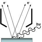
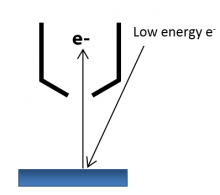
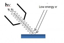
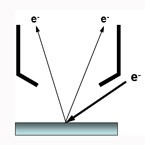
It is the surface, or outermost layer of atoms of a solid, that will really define how that material interacts with is surroundings and how it behaves for its intended purpose.  In fact, the surface of a solid is perhaps the most important region of the material.  For example, it will define the materials' adhesive properties.  Will something stick to that surface such as a protective coating to prevent corrosion or reduce the ability of small cells to adhere and form biofilms?  In this article the importance of surfaces in materials science is highlighted along with important analytical techniques available to characterise those surfaces.

Ultraviolet Photoemission Spectroscopy (UPS)

Ultra violet photoemission spectroscopy (UPS) is analogous to XPS but the excitation source is a helium discharge source.  Depending on the operating conditions of the source the photon energy can be optimised for He I = 21.22eV or He II = 40.8eV which is significantly lower energy than Al or Mg Kα used in XPS.  This technique measures the valence electrons and can be used to determine the sample work function. 

Information content from UPS experiments

  • Investigation of valence band and highest molecular orbitals
  • work function measurements of materials

Reflection electron energy loss spectroscopy (REELS)

Electron energy loss spectroscopy (EELS) involves the exposure of the sample to a focused beam of monoenergetic electrons, typically < 3keV.  As these electrons interact with the material some of them will undergo inelastic scattering whereby they lose some kinetic energy.  The REEL spectrum can be used to determine information about the band structure and dielectric properties of the sample. 

Information content from REELS experiments

  • Probe surface valence and conduction band electronic properties.
  • Band gap determination for semiconductor materials.
  • Comparison of relative hydrogen content in polymer materials.
  • Investigation of conjugation or aromaticity in organic materials.
  • Determination of sp2 / sp3 hybridisation of carbon

Inverse photoemission spectroscopy (IPES)

As the name suggests, the technique of inverse photoemission spectroscopy (IPES) is the opposite of the much more common photoemission (XPS) process.  It relies on incident low energy electrons interating with a materials unoccupied orbitals in the conduction band.  As these electrons make the direct transition to fill the unoccupied states the photons that are emitted are measured.  

Auger Electron Spectroscopy (AES)

Auger electron spectroscopy (AES) employs a beam of electrons as surface a probe. As a result of electronic rearrangements within the atoms, Auger electrons characteristic of each element present at the surface are emitted from the surface.   Since the probe electrons can be focused to diameters <0.5μm high spatial resolution analysis (scanning Auger microprobe, SAM) can be performed.  Rastering the focused electron beam synchronously with a video display, using scanning electron microscope (SEM) techniques, produces physical images and element distribution maps of the surface.