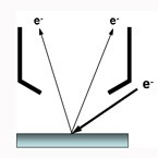
AES employs a beam of electrons as surface a probe. As a result of electronic rearrangements within the atoms, Auger electrons characteristic of each element present at the surface are emitted from the surface. Only those electrons that emerge from the topmost atomic layers contribute to the spectrum so giving rise to the high surface specificity of this technique. Auger electron spectroscopy (AES) detects all elements except hydrogen and helium usually to a sensitivity better than 1 atom percent of a monolayer. Since the probe electrons can be focused to diameters <0.5μm high spatial resolution analysis (scanning Auger microprobe, SAM) can be performed. Rastering the focused electron beam synchronously with a video display, using scanning electron microscope (SEM) techniques, produces physical images and element distribution maps of the surface. The ability to pinpoint exact areas for analysis makes AES especially suited to investigations of the small features of microelectronic circuits or very fine surface particles.
The AXIS Supra+ can be configured with a 10 keV FE-electron source for AES, SEM and SAM.